Purpose
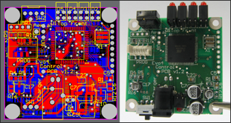
Printed Circuit Boards (PCB’s) are used in electronic components to both mechanically support and provide electrical connections between components. Construction involves etching a thin copper layer that has been deposited onto a non-conductive, glass-fiber/epoxy composite substrate. Electrical components are then mounted to the board and connected to the copper traces with electrical solder.
The concentrated, intense heating that occurs during the soldering process creates stresses in the substrate material. In this exercise, you will simulate this process and determine if the stresses and strains resulting from this process are acceptable or not.
The model makes use of solid hexahedral (CHEXA8) elements with a thin skin of shell elements (CQUAD4) on the outside faces.
The consistent unit system used in this simulation are: kg, mm, GPa, kN and °C
Problem Statement
In this tutorial, you learn how to:
| • | Create MAT2 and MAT9 material definition cards |
| • | Create PSOLID and PSHELL element property cards |
| • | Create applied temperature loads and constraints (TEMP and SPC cards) |
| • | Create a temperature loading subcase |
| • | Request strain output with the STRAIN control card |

Exercise
Step 1: Launch HyperMesh and set the OptiStruct User Profile
| 1. | Launch HyperMesh. The User Profiles dialogs appears. |
| 2. | Select OptiStruct and click OK. This loads the user profile. It includes the appropriate template, macro menu, and import reader, paring down the functionality of HyperMesh to what is relevant for generating models for OptiStruct. |
Step 2: Open the File circuit_board.hm
| 1. | Click File > Open. An Open Model browser window opens. |
| Note: | If HyperMesh Desktop was launched, use: File > Open > Model. |
|
| 2. | Select the circuit_board.hm file you saved to your working directory from the optistruct.zip file. Refer to Accessing the Model Files. |
| 3. | Click Open. The circuit_board.hm database is loaded into the current HyperMesh session, replacing any existing data. The database only contains geometric data. |
Step 3: Create a MAT9 material definition for the solid elements
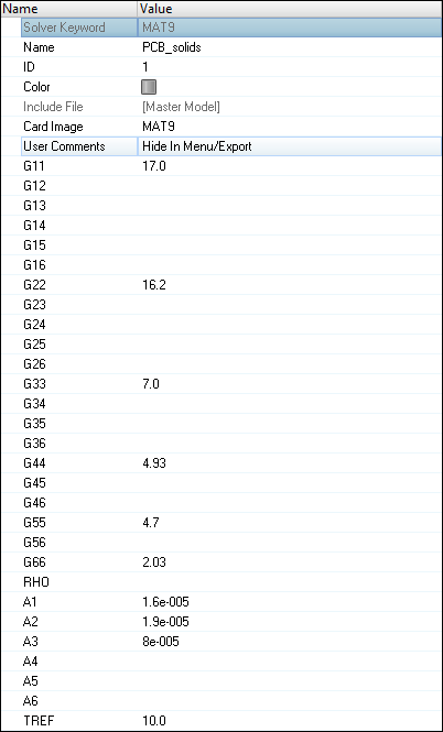
The MAT9 material type defines the properties for linear, temperature independent, anisotropic materials. This material model is well suited to this tutorial, due to the composite structure of the substrate. The X, Y and Z orientations of the laminated material have different elastic moduli and thermal expansion coefficients. The MAT9 material applied to solid elements allows a simplification of the model over using a shell model of the composite, with the individual ply layer properties and orientations defined.
| 1. | In the Model browser, right-click and select Create > Material. |
| 2. | For Name, enter PCB_solids. |
| 3. | For Card Image,select MAT9 and click Yes to confirm. |
| 4. | Enter the following values for the oriented elastic and shear modulus of the composite: |
G11
|
G22
|
G33
|
G44
|
G55
|
G66
|
17.0
|
16.2
|
7.00
|
4.93
|
4.70
|
2.03
|
| 5. | Enter the following values for the thermal expansion rates and reference temperature: |
A1
|
A2
|
A3
|
TREF
|
1.6e-5
|
1.9e-5
|
8.0e-5
|
10.0
|

Step 4: Create a MAT2 material definition for the shell elements
You should still be in the materials/create panel from the previous step.
| 1. | In the Model browser, right-click and select Create > Material. |
| 2. | For Name, enter PCB_shells. |
| 3. | For Card Image, select MAT2 and click Yes to confirm. |
| 4. | Enter the following values for the shell element material properties: |
G11
|
G22
|
G33
|
A1
|
A2
|
TREF
|
17.0
|
16.2
|
4.90
|
1.6e-5
|
1.9e-5
|
10.0
|
Step 5: Create properties with a material reference and update the existing components
| 1. | In the Model browser, right-click and select Create > Property. |
| 3. | For Card Image, select PSHELL. |
| 4. | For Material, click Unspecified > Material. |
| 5. | In the Select Material dialog, select PCB_shells from the list of materials and click OK to complete the material selection. |
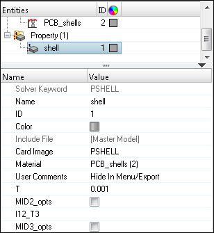
| 6. | Enter the thickness for the shell component by clicking T, and enter 0.001. |

| 7. | Repeat steps 1 to 6 to create another property with name Solids, with Card Image set as PSOLID and Material as PCB_solids. |
| 8. | In the Model browser, click the pcb_solids component. The component entry is displayed in the Entity Editor below. |
| 9. | For Property, click Unspecified > Property. |
| 10. | In the Select Property dialog, select Solids and click OK to complete the property selection. |
| 11. | Repeat steps 8 to 10 for both solder_pads and shell_faces selecting shell for the property name. |
Step 6: Create displacement constraints at the mounting holes
| 1. | In the Model browser, right-click and select Create > Load Collector. |
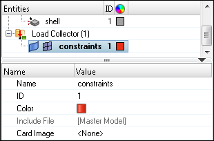
| 2. | For Name, enter constraints. |
| 3. | Leave Card Image set to None. |
| 4. | Select a suitable color. |

| 5. | Click BCs > Create > Constraints to open the Constraints panel. |
| 7. | Select the constrain_nodes entity set and click select. |
| 8. | Leave all 6 degrees of freedom selected and click create. |
| 9. | Click return to go back to the main menu. |
Step 7: Create applied temperature loads at the solder pad locations
| 1. | Create a new load collector named temperature_loads. |
| 2. | Leave Card Image set to None. |
| 3. | Click BCs > Create > Temperatures to open the Temperatures panel. |
| 4. | Click nodes > by collector. |
| 5. | Check the box next to the solder_pads component. |
| 7. | Verify that constant value (the field label specifies value=) is selected and enter 345.0. |
| 8. | Verify the load types= is set to TEMP. |
| 9. | Click create to create the temperature_loads. |
| 10. | Click return to go back to the main menu. |
Step 8: Create a thermal stress analysis subcase
| 1. | In the Model browser, right-click and select Create > Load Step. |
| 2. | For Name, enter thermal_loading. |
| 3. | Set the Analysis type to Linear Static. |
| 4. | For SPC, click Unspecified > Loadcol. |
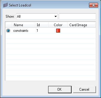
| 5. | In the Select Loadcol dialog, select constraints from the list of load collectors and click OK to complete the selection. |

| 6. | For TEMP, click Unspecified > TEMP. |
| 7. | In the Select Loadcol dialog, select temperature_loads from the list of load collectors and click OK to complete the selection. |
Step 9: Add OUTPUT, STRAIN and SCREEN control cards to the analysis deck
| 1. | Click Setup > Create > Control Cards to open the Control Cards panel. |
| 2. | Click next to advance until OUTPUT is available, click OUTPUT to add card requesting output results format. |
| 3. | For the number_of_outputs field on the lower part of the panel, enter 2. |
| 4. | Set one of the KEYWORD to OP2 to request the OP2 format results file, and set the second output as H3D format. The frequency (FREQ) of the output can be set as ALL. |
| 5. | Click return to go back to the Control Cards panel. |
| 6. | Click next to advance to the second page of control cards, then once more to go to the third page. |
| 7. | Activate the SCREEN card with the OUT option. |
| 8. | Then return to the Control Card panel. |
| 9. | Select GLOBAL_OUTPUT_REQUEST on the first page to access the output settings. |
| 10. | Activate the STRAIN option to request strain results output. Leave the default settings for this card. |
| 11. | Click return twice to get back to the main menu. |
Step 10: Run the analysis and review the results
| 1. | From the Analysis page, enter the OptiStruct panel. |
| 2. | Click Save as and enter the file name as <your_file_name>.fem. |
| 3. | Click OptiStruct to submit the job. |
| 4. | Once the job has completed, the results can be reviewed in HyperView. |
See Also:
OptiStruct Tutorials


